- 您现在的位置:买卖IC网 > Sheet目录502 > QS6K1TR (Rohm Semiconductor)MOSFET 2N-CH 30V 1A TSMT6
QS6K1
Transistors
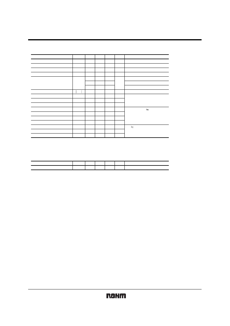
Electrical characteristics (Ta=25 ° C)
<It is the same characteristics for the Tr1 and Tr2>
Parameter
Gate-source leakage
Symbol
I GSS
Min.
?
Typ.
?
Max.
10
Unit
μ A
Conditions
V GS = 12V, V DS = 0V
Drain-source breakdown voltage V (BR) DSS
30
?
?
V
I D = 1mA, V GS = 0V
?
Zero gate voltage drain current
Gate threshold voltage
Static drain-source on-state
resistance
I DSS
V GS (th)
R DS (on)
?
0.5
?
?
?
?
?
170
180
260
1
1.5
238
252
364
μ A
V
m ?
V DS = 30V, V GS = 0V
V DS = 10V, I D = 1mA
I D = 1.0A, V GS = 4.5V
I D = 1.0A, V GS = 4.0V
I D = 1.0A, V GS = 2.5V
Forward transfer admittance
Input capacitance
Output capacitance
Reverse transfer capacitance
Turn-on delay time
Rise time
Turn-off delay time
Fall time
Y fs
C iss
C oss
C rss
t d (on)
t r
t d (off)
t f
?
?
?
?
?
1.0
?
?
?
?
?
?
?
?
77
25
15
7
7
15
6
?
?
?
?
?
?
?
?
S
pF
pF
pF
ns
ns
ns
ns
I D = 1.0A, V DS = 10V
V DS = 10V
V GS = 0V
f = 1MHz
I D = 500mA, V DD 15V
V GS = 4.5V
R L = 30.0 ?
R G = 10 ?
Total gate charge
Q g
?
?
1.7
2.4
nC
V DD
15V
Gate-source charge
Gate-drain charge
Q gs
Q gd
?
?
?
?
0.4
0.4
?
?
nC
nC
V GS = 4.5V
I D = 1.0A
? Pulsed
Body diode characteristics (Source-Drain) (Ta=25 ° C)
<It is the same characteristics for the Tr1 and Tr2>
Parameter
Forward voltage
Symbol
V SD ?
Min.
?
Typ.
?
Max.
1.2
Unit
V
Conditions
I S = 3.2A, V GS = 0V
? Pulsed
Rev.B
2/3
发布紧急采购,3分钟左右您将得到回复。
相关PDF资料
QS6K21TR
MOSFET N-CH 45V 1A TSMT6
QS6M3TR
MOSFET N+P 30,20V 1.5A TSMT6
QS6M4TR
MOSFET N+P 30,20V 1.5A TSMT6
QS6U22TR
MOSFET P-CH 20V 1.5A TSMT6
QS6U24TR
MOSFET P-CH 30V 1A TSMT6
QS8K2TR
MOSFET 2N-CH 30V 3.5A TSMT8
QSB320FTR
PHOTOTRANSISTOR IR 880NM 2-PLCC
QSB34
PHOTODIODE GULL WING SMD
相关代理商/技术参数
QS6K21
制造商:ROHM 制造商全称:Rohm 功能描述:2.5V Drive Nch MOSFET
QS6K21TR
功能描述:MOSFET Med Pwr, Sw MOSFET N Chan, 45V, 1A RoHS:否 制造商:STMicroelectronics 晶体管极性:N-Channel 汲极/源极击穿电压:650 V 闸/源击穿电压:25 V 漏极连续电流:130 A 电阻汲极/源极 RDS(导通):0.014 Ohms 配置:Single 最大工作温度: 安装风格:Through Hole 封装 / 箱体:Max247 封装:Tube
QS6M3
制造商:ROHM 制造商全称:Rohm 功能描述:Small switching
QS6M3_1
制造商:ROHM 制造商全称:Rohm 功能描述:2.5V Drive Nch+Pch MOSFET
QS6M3TR
功能描述:MOSFET N+P 30 20V 1.5A TSMT6 RoHS:否 制造商:STMicroelectronics 晶体管极性:N-Channel 汲极/源极击穿电压:650 V 闸/源击穿电压:25 V 漏极连续电流:130 A 电阻汲极/源极 RDS(导通):0.014 Ohms 配置:Single 最大工作温度: 安装风格:Through Hole 封装 / 箱体:Max247 封装:Tube
QS6M4
制造商:ROHM Semiconductor 功能描述:MOSFET,Pch(20V)Nch(30V),1.5A2,TSMT6
QS6M4_1
制造商:ROHM 制造商全称:Rohm 功能描述:2.5V Drive Nch+Pch MOSFET
QS6M4TR
功能描述:MOSFET N+P 30 20V 1.5A TSMT6 RoHS:否 制造商:STMicroelectronics 晶体管极性:N-Channel 汲极/源极击穿电压:650 V 闸/源击穿电压:25 V 漏极连续电流:130 A 电阻汲极/源极 RDS(导通):0.014 Ohms 配置:Single 最大工作温度: 安装风格:Through Hole 封装 / 箱体:Max247 封装:Tube
